
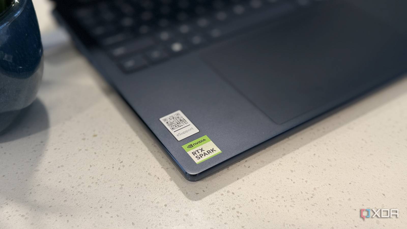
Published Oct 30, 2026, 7:00 AM EDT I’m Adam Conway, an Irish technology fanatic with a BSc in Computer Science and I'm XDA’s Lead Technical Editor. My Bachelor’s thesis was conducted on the viability of benchmarking the non-functional elements of Android apps and smartphones such as performance, and I’ve been working in the tech industry in some way or another since 2017. In my spare time, you’ll probably find me playing Counter-Strike or VALORANT, and you can reach out to me at adam@xda-developers.com, on Twitter as @AdamConwayIE, on Instagram as AdamConwayIE, or u/AdamConwayIE on Reddit. Sign in to your XDA account When Nvidia announced its RTX Spark earlier this year, everything we learned pointed to this chip being extremely similar, if not practically identical, to the GB10 launched alongside the DGX Spark last year, except this time around it's only available for Windows-based machines. I've been testing an HP OmniBook Ultra 16 with the RTX Spark over the past couple of weeks, and while that assertion is essentially true, there are some differences when you look further than the spec sheet. In my testing, I found that both HP's laptop and Nvidia's DGX Spark report the same SoC ID, the same CPU cores, the same GPU, and firmware that describes the same hardware complete with the same individual register addresses. However, in pracitce, there are also some significant differences. Not only does the RTX Spark run its memory faster, its firmware enables hardware that GB10 boards leave switched off. On top of that, Windows handles the shared memory pool very differently to Linux. When running benchmarks on both devices, using identical GPU and CPU tests, the compute difference is often within a percent or two of each other. When they do differ, it tends to be the laptop coming out ahead, especially in tasks bound by memory bandwidth. And memory bandwidth matters enormously when running local LLMs. The RTX Spark and the GB10 say they're the same silicon Right down to the memory map The obvious first step was to check whether the two chips identify themselves the same way, and they do. Both say they're SoC revision 0x04268901, both pack ten Arm Cortex-X925 performance cores and ten Cortex-A725 efficiency cores, and both split those cores across two clusters in the same order, complete with matching 8 MB and 16 MB L3 caches. Their GPUs also report identical specifications: 48 SMs, CUDA compute capability 12.1, 24 MiB of L2 cache, and a maximum clock of 3,003 MHz. Nvidia's driver code handles both in an identical fashion, and the company's open kernel driver identifies the GB10's GPU internally as GB20B, which is the same identifier used by the RTX Spark. In firmware there's a similar story, with both devices describing the SoC's on-die peripherals at the same physical addresses, even using near-identical device names in their ACPI tables, and these are what tells the operating system about the hardware and how to use it. Both Lenovo's GB10 firmware and HP's RTX Spark firmware even refer to a device as NH1X, which looks an awful lot like "N1X." I couldn't establish what this is given that there's no driver bound to it and neihter machine assigns it resources. The PCI device IDs line up with this interpretation too, with the GB10's GPU identifying as 10DE:2E12 and the RTX Spark's GPU identifying as 10DE:2E03. On top of that, in Nvidia's published porting guide, the desktop variant of the RTX Spark is listed as 10DE:2E13, just one hexadecimal digit away from GB10. It's not proof, but everything aligns very neatly between the two. What we can already say from this is that Nvidia is shipping a single chip design under two names, but we can't say whether some parts have been fused off of the die on either SKU. In fact, the major differences that I've seen all down to what each board's firmware and operating system choose to use. The laptop has faster memory, and it shows 9,400 MT/s versus 8,533 Both of these machines have 128GB of LPDDR5X on a 256-bit bus, but they're running at different speeds. On the HP OmniBook Ultra 16, its memory runs at 9,400 MT/s compared to the DGX Spark's 8,533 MT/s. That's roughly 300 GB/s of theoretical bandwidth on the RTX Spark compared with 273 GB/s on the GB10, and this is most obvious in operations that saturate memory bandwidth. This gap, though, is even bigger than those numbers may suggest. I conducted a GPU read test over a 2 GB buffer, hitting 282.9 GB/s on the RTX Spark and 239.8 GB/s on the GB10, which is an 18% lead for the laptop rather than the 10% the spec sheet would predict. The RTX Spark reached 94% of its theoretical bandwidth, while the PGX only managed 88%. I first suspected that this was caused by the method each OS allocates GPU memory, but repeating the test with a buffer explicitly allocated using 2 MB pages on both machines didn't help. That test gave me 281 to 285 GB/s on the RTX Spark and 243 to 244 GB/s on the GB10, leaving practically the same gap. Page size alone doesn't explain the difference, and I wasn't able to isolate the speed improvement down to something like memory timings, fabric clocks, drivers, or something else. The same goes for the CPU, where a single thread can pull 45.0 GB/s on both machines in a STREAM triad test, but with all 20 cores loaded, the RTX Spark can get to 142.5 GB/s compared with 116.2 GB/s on the GB10, roughly 23% higher. There's something more than memory speed going on here, though this test could have been caused by something like thread placement on the OS's scheduler. Latency swings the other way though. From a performance core, a pointer-chasing test across a 1 GB working set, on the RTX Spark managed 134.5 ns, compared with 131.1 ns on the GB10. Switching to an efficiency core, however, saw the RTX Spark lag significantly behind, coming in at 204 ns compared with 162 ns. Some of this could come down to power management and memory fabric clock speeds being kept at a lower clock under light workloads. I found an Nvidia engineer on the company's developer forums outlining how the GB10's efficiency cores can clock down as low as 330 MHz, but that the performance governor can effectively disable deeper CPU sleep states. That could help explain the DGX's lower latency. Bandwidth is what really matters for local LLMs, as token generation is largely limited by how quickly the GPU can read the model's weights from memory. Using Qwen 3.8 Flash Next quantized to Q4_K_M in llama.cpp, roughly 4.6 GB of weights get read for every token, which sets a theoretical ceiling of approximately 58 tokens per second on the RTX Spark and 49 on GB10, based on my measured bandwidth. On OmniBook Ultra, using llama.cpp and multi-token prediction, I get about 45 tokens per second in actual use, and the same model comes in at roughly the same or a bit lower on the DGX Spark, which serves it through vLLM. Neither is faster at raw compute, and FP16 tensor throughput comes in at 123.9 TFLOPS on the RTX Spark and 124.3 TFLOPS on the GB10. FP8 comes in at around 250 TFLOPS, INT8 at around 250 TOPS, and FP32 at 29.56 versus 29.83 TFLOPS. Aiming for Nvidia's "1 PFLOP of FP4" is achievable when using 2:4 structured sparsity, and the GB10 reaches 1,002.7 TFLOPS while the RTX Spark reaches 989.6. Dense FP4 throughput is about half that on both. GeForce cards have historically run FP16 tensor operations with FP32 accumulation at half rate, so I wanted to test that next. The RTX Spark identifies itself as a GeForce product, while GB10 reports as Nvidia RTX, and the restriction doesn't apply to either. Sustained performance between the two was quite close, and over a 60-second FP16 load, both GPUs settled at around 2.52 to 2.56 GHz and drew between 44 and 49 W, with a median of approximately 123 TFLOPS on the OmniBook and 124.6 TFLOPS on the DGX Spark. The laptop ran five to ten degrees hotter at the same power, peaking at 71°C, and showed one quirk that the DGX Spark didn't. When I ran repeated runs of this test, the RTX Spark would sometimes score approximately 7% lower. Both chips are rated for very different power consumptions, and Nvidia gives the GB10 a 140 W TDP for the whole SoC, with a 240 W power supply in the DGX Spark, while RTX Spark laptops are rated at 45 to 80 W. The desktop variant of the RTX Spark does share the GB10's 140 W figure, though. Sadly, there's no power limit exposed in nvidia-smi, so I can't see what HP has actually configured. All I know is that, in my sustained CPU and GPU test, the CPU stayed maxed out, whereas the GPU dropped from approximately 48W to 34W. The CPU itself is quite interesting, as the RTX Spark's X925 cores run about 100 MHz faster, at 4.0 to 4.1 GHz against 3.9 to 4.0 GHz on the GB10. When all 20 cores are loaded for a minute, the RTX Spark's performance cores maintained a steady speed between 3.86 GHz and 4.0 GHz. Meanwhile, the DGX Spark managed to maintain between 3.86 GHz to 3.9 GHz. Single-core FP64 throughput on an X925 was 97.3 GFLOPS on the RTX Spark and 91.6 on the GB10, while the A725 cores were identical. Both systems also report slightly different CPU features, though this is likely caused by Windows running on top of Hyper-V with virtualization-based security enabled. Windows doesn't show BTI, MTE, and a few other Arm extensions that Linux on the GB10 reports, The core identification registers are otherwise identical, and I found no evidence that either firmware is hiding CPU features. It's a carveout on Windows, but a free for all on Linux Both the RTX Spark and the GB10 use a single unified pool of memory shared between the CPU and the GPU, but how that memory is allocated differs wildly between Windows and Linux. On the GB10 when running Linux, it's a complete free for all with CUDA reporting the full system memory available, allowing the GPU to allocate memory using the entire pool if needed. Things are significantly different on Windows with the RTX Spark, though, where a chunk up to 96 GB is reserved as "dedicated" GPU memory. CUDA still sees a full 109.7 GB available for allocation no matter what you reserve, but it changes how much Windows can use as system memory. When I ran my benchmarks, I had set the dedicated memory to 84.5 GB, and Windows reported 41 GB of system memory available. The GB10's UEFI also reserves 2 GB of memory for the display, and that memory is not made available to the OS, CUDA, or other applications. In the OTA2610 update, this changed, and the reservation can be set to 0.5, 1, 2, 4, or left on Auto. There's no equivalent in the RTX Spark firmware, which I confirmed by looking at its UEFI variables. The system reservation used to be 4 GB, and an engineer at Nvidia engineer stated that it had been reduced to 2 GB in a firmware update. The Lenovo ThinkStation PGX doesn't have that update, seeing a reserved 4 GB memory portion compared with 2 GB on my DGX Spark. As a result, Linux sees 119.6 GiB on the PGX compared with 121.7 GiB on the DGX Spark. These two memory models behave differently for developers; for example, memory copies between host and device are more than twice as fast on the RTX Spark with Windows, at 132.7 GB/s versus 59.4 GB/s on the GB10 with Linux. The RTX Spark's GPU can also read pinned host memory at 278.5 GB/s, close to its full memory bandwidth. On the other hand, Linux lets the GPU read ordinary memory allocated by the CPU without registering it first, reaching 168.3 GB/s in my test, and Windows doesn't support that at all. CUDA's managed memory, where the runtime manages CPU and GPU access to allocations, was faster on the GB10 too, at 163.4 GB/s against 103.0 GB/s. There are a few CUDA features that present differently, too. The DGX Spark says that it supports concurrent managed memory access and direct access to pageable memory, yet the RTX Spark does not. As well, Nvidia's RTX Spark porting guide also tells developers to avoid managed memory on Windows because of the performance costs of its compatibility path. Neither of these two chips support GPUDirect RDMA, which allows a PCIe device like a network card to read and write GPU memory directly, and dma-buf isn't supported either. That's more surprising on the GB10, as it's the one with ConnectX-7, but Nvidia's DGX Spark porting guide confirms it while also saying that nvidia-peermem and GDRCopy don't work either. The problem comes from the fact that memory allocated with cudaMalloc can't be coherently accessed by the CPU or PCIe devices, so RDMA applications need to use pinned host buffers allocated with cudaHostAlloc and registered with the network card instead. Clustering still works, and the difference is that RDMA transfers have to use those pinned host buffers rather than ordinary CUDA device allocations. Each board's features are defined by firmware Same plumbing, different switches The biggest differences between the two are really defined by what the platform's firmware enables, with USB-C being the clearest example. The specifications across GB10-powered devices are inconsistent, though. While Nvidia's DGX Spark porting guide names USB 3.2 driver support and says that "dGPU attach" is unsupported, Lenovo's spec sheet for the ThinkStation PGX says that its power-input port is "USB 20Gbps / USB4" while saying that the other three are 20Gbps USB 3.2 Gen 2x2. What I actually see on my GB10 devices are USB 3.2 ports, though the USB4 hardware is actually there. Analyzing the DGX Spark's early-boot log, I can see that it loads and initializes a dedicated USB4 firmware image, and the firmware on both the ThinkStation PGX and the DGX Spark describe four USB4 routers, one per USB-C port, each paired with its own PCIe tunnelling port. All four are disabled before the OS starts up, and Linux brings the ports up as 20Gbps USB 3.2 Gen 2x2 controllers with no USB4 bus to talk to. The RTX Spark in the HP enables two of those routers, enabling Windows to load its USB4 stack, and PCIe tunnelling works. I had often seen an explanation given that pinned the blame on the GB10 running out of PCIe lanes, given that it uses a lot of them on networking. However, Nvidia's Hot Chips presentation on the GB10 lists eight PCIe Gen5 lanes going to ConnectX-7, the high-speed NIC used for clustering Spark devices, which is split into two x4 links because the SoC can't provide more than x4 per device. These USB4 tunnelling ports are separate controllers attached to the USB4, and they don't use those external PCIe links. HP's laptop doesn't have ConnectX-7, with one x4 link switched off and the other carrying the SSD. There are also two USB4 PCIe tunnels working alongside them. Of course, I can't establish what the physical wiring is doing from the software alone, but nothing I've found in the firmware or operating systems suggests that USB4 tunnelling and ConnectX-7 are competing for the same lanes. Instead, what separates these two things is the firmware. HP's firmware has per-port settings for USB4 link speed and PCIe tunnelling, both enabled by default and neither exposed in its BIOS menu, and a USB4 router is only enabled when its corresponding port is configured for USB4. Nvidia's and Lenovo's GB10 firmware doesn't have those settings at all, and the table disabling PCIe tunnelling is identical on both machines. All of this points to a decision made in Nvidia's reference firmware. There's one likely reason for this: Linux. Nvidia's GB10 USB4 routers aren't PCI devices like what you'd find in Thunderbolt and USB4 controllers on AMD or Intel. Instead, they're blocks described to the OS through ACPI. Historically speaking, Linux has generally assumed that the Thunderbolt and USB4 driver's host router is a PCIe device, so nothing in the kernel can even bind to the controllers described by its firmware. Windows, meanwhile, has a driver capable of handling this kind of route. Support for non-PCIe USB4 hosts on Linux is still in the works, and in May 2026, Konrad Dybcio submitted patches to remove the driver's assumption that the host router must be a PCIe device. These tested on a Qualcomm Snapdragon X Elite reference design, where the controllers face a similar problem. Over there, USB4 works on Windows while Linux support is still being developed. DGX OS is based on Linux, so even if I had enabled the GB10's routers, the existing USB4 driver wouldn't have been able to use it anyway. Disabling USB4 was still a choice made by Nvidia, seeing as the company could have written its own driver. However, given the state of Linux support, it's an understandable choice to make. I haven't found evidence of anything wrong with the USB4 hardware in GB10 itself, but I can't rule out additional platform or firmware limitations. Connecting the Plugable Thunderbolt 5 enclosure with a Gigabyte RTX 4080 reveals another limitation, though. In this setup, the PCIe tunnel came up and the card even enumerated at Gen4 x4 over a 40Gbps USB4 link (Gen 3, dual lane). Windows could see it... but it couldn't use it. Nvidia's Arm64 doesn't support other GPUs aside from the RTX Spark's own device IDs, causing Windows to fall back to its Basic Display Adapter, which also fails to start with a Code 10 error and the message "The driver trying to start is not the same as the driver for the POSTed display adapter." Right now, you need Arm64 drivers to use an eGPU, and on a GB10 machine, you can't even get as far as a PCIe tunnel. As for the NPU, the RTX Spark exposes something like a descendant of Nvidia's Deep Learning Accelerator, showing up as "NVIDIA NPU" in Device Manager and as a second device in nvidia-smi. I was able to run real neural networks running on it with correct results, but the GB10 doesn't expose an equivalent device. Its firmware never defines a DLA device for Linux to find, and the DGX Spark porting guide mentions DLA in its chip features table while marking it "NO." The DGX Spark's early-boot firmware log explicitly records the DLA as disabled. It's unclear if that hardware, should it exist on the GB10, could ever be switched on, and I've had no luck trying. On the RTX Spark, software support is still sorely lacking. DaVinci Resolve's Windows on Arm build packs Qualcomm's SNPE with a backend for Qualcomm's NPU, and Blackmagic says it can improve the speed of AI tools like Magic Mask up to 4.7x faster. Nvidia doesn't have a corresponding backend, meaning that this isn't available for the RTX Spark. Resolve can still do all of its AI processing on the GPU, but that's quite different from being able to use a dedicated low-power accelerator. Aside from that, each platform enables the SoC blocks it needs. The RTX Spark enables the chip's I2C controllers and its SoundWire audio controller, the latter of which Nvidia's DGX Spark porting guide lists as unsupported on GB10. As well, both chips have a security processor at the same physical address that Windows uses for Microsoft's Pluton. However, Linux on the GB10 doesn't use it at all, with Nvidia's porting guide stating that the GB10 relies on a separate TPM chip. Finally, the GB10's firmware identifies several blocks, such as the serial port and the power management controller, with MediaTek identifiers, as MediaTek co-designed the chip. The RTX Spark's firmware names the same blocks as Nvidia devices. Windows gets the more complete driver stack For now, anyway The RTX Spark Windows driver comes from a significantly newer branch than what you get in DGX OS, and you can see it in the feature list. Vulkan on the RTX Spark exposes 290 device extensions against 249 on the GB10, though major features are shared across them. This includes ray tracing, mesh shaders, cooperative matrices, and Vulkan Video encoding and decoding. Most of the extras are newer extensions, with a handful specific to each operating system. There are some oddities though, like optical flow which is exposed on Windows but not Linux. The hardware engine is present on both chips. Gaming is where things will change a lot; on the ThinkStation PGX, getting Cyberpunk 2077 running meant using FEX-Emu to translate x86 instructions, Proton to translate DirectX to Vulkan, and copying x86 Nvidia libraries into FEX's root filesystem just to get DLSS working. The RTX Spark's driver works with Direct3D, Vulkan, and NVAPI components as native Arm64 and Arm64EC builds. That means an x64 game running under Windows' Prism emulation can still use native driver code, while DLSS and Frame Generation models are also available in Arm64 versions. There's significantly less overhead to get games running on this, even if the games still need to be translated. To test this, I ran the same Cyberpunk 2077 tests that I ran on Lenovo's ThinkStation PGX, which were using a 2560*1440 monitor and on the Ultra preset. In that test, I was able to achieve an average FPS of 61.75 with a minimum FPS of 48.38. The HP OmniBook Ultra 16, set to 2560*1440, achieved 65.13 FPS with a minimum of FPS of 52.60. It's a small improvement, but it's an improvement nonetheless. Nvidia's RTX Spark driver still brings along some Linux with it, too. The 617.42 driver comes with Arm64 Linux libraries and tools for WSL, including libcuda, nvidia-smi, and the D3D12 driver WSL uses for graphics. They're built from Nvidia's 617 branch, which is newer than the publicly released 615 Linux branch, while DGX OS on my DGX Spark is still on 580.178.04. This means that RTX Spark laptops come with newer Linux user-space drivers than the GB10 itself gets. Nvidia's later changed its 12K video claim Blackmagic is doing the heavy lifting The video hardware across both chips is the exact same, with one NVENC and one NVDEC each. Windows supports asynchronous encoding where Linux doesn't, and the newer driver allows more B-frames, but neither of those differences are from the SoC itself. The decoder on both chips reports the same supported formats, including the 10-bit 4:2:2 H.264 and HEVC decoding that Blackwell added, with a maximum resolution of 8192*8192. There's one problem with that limit: it doesn't match Nvidia's original claim from back in May that the RTX Spark can "edit 12K 4:2:2 video with the NVIDIA Blackwell decoder." Nvidia's own Video Codec SDK documentation states that 8192*8192 is Blackwell's maximum decoding resolution, which matches what both chips say they're capable of, and a 12K frame is 12,288 pixels wide. Nvidia later published a press release that only claims 8K 4:2:2 video support, which makes a lot more sense. Still, I opted to give the original claim a shot with a 12K Blackmagic RAW video file. Blackmagic's SDK decodes using the CPU or GPU compute cores rather than NVDEC, but I still wanted to test the original claim. Blackmagic has optimized its CPU decoder for 12K clips, and I was able to open Blackmagic's "big sensor magic" sample, a 4.6GB, 12,288*8,040 BRAW clip, at full resolution in DaVinci Resolve on the laptop. With GPU decoding enabled, playback was smooth, GPU utilization sat at 7 to 8%, and CPU usage stayed between 6 and 7%. Disabling GPU decoding didn't introduce any stuttering either, though CPU usage climbed to between 26 and 29%. This is Looking at Resolve's Windows on Arm build, it's a mix of native and emulated code. Resolve and its Blackmagic RAW decoder are Arm64EC binaries that run natively, while many third-party libraries, including FFmpeg and ARRI's SDK, are still x64 and run with Microsoft's Prism. What's important here is that Blackmagic RAW decoding path runs natively, and the RTX Spark can play full-resolution 12K footage smoothly without relying on NVDEC. The same CPU and GPU hardware in the GB10 should be capable of similar decoding performance, provided the software is available and properly supported. Two similar SoCs, two different implementations And for very different people After spending so much time with the RTX Spark and the GB10, I feel confident in saying that they are the same chip. Even still, calling the RTX Spark a "GB10 with Windows" slightly undersells what Nvidia has done here. It has memory that runs faster, a CPU that's clocked a little bit higher, enables PCIe tunnelling, and has an NPU that GB10 boards either switch off or leave out entirely. The GB10 has its own advantages in ConnectX-7 and a Linux memory model that lets the GPU allocate from the entire available memory pool. For many CUDA developers, that second point alone probably matters a whole lot more than an 18% bandwidth lead. What this demonstrates is that these machines are clearly aimed at different people. The DGX Spark with its GB10 (along with all of the other GB10 machines) are the ones people will have fine-tuning models or permanently serving models using inference servers like vLLM, whereas the laptop is still a laptop. It's just a little odd that the laptop is the one with faster memory and an NPU.
Nvidia's RTX Spark laptops use the same chip as the DGX Spark, but they get faster memory and features the DGX Spark doesn't
Full Article
Original Source
Read the full article at Xda-developers →KhanList aggregates and links to publicly available news content. We do not host full articles from third-party sources. Always verify important information with original sources.