
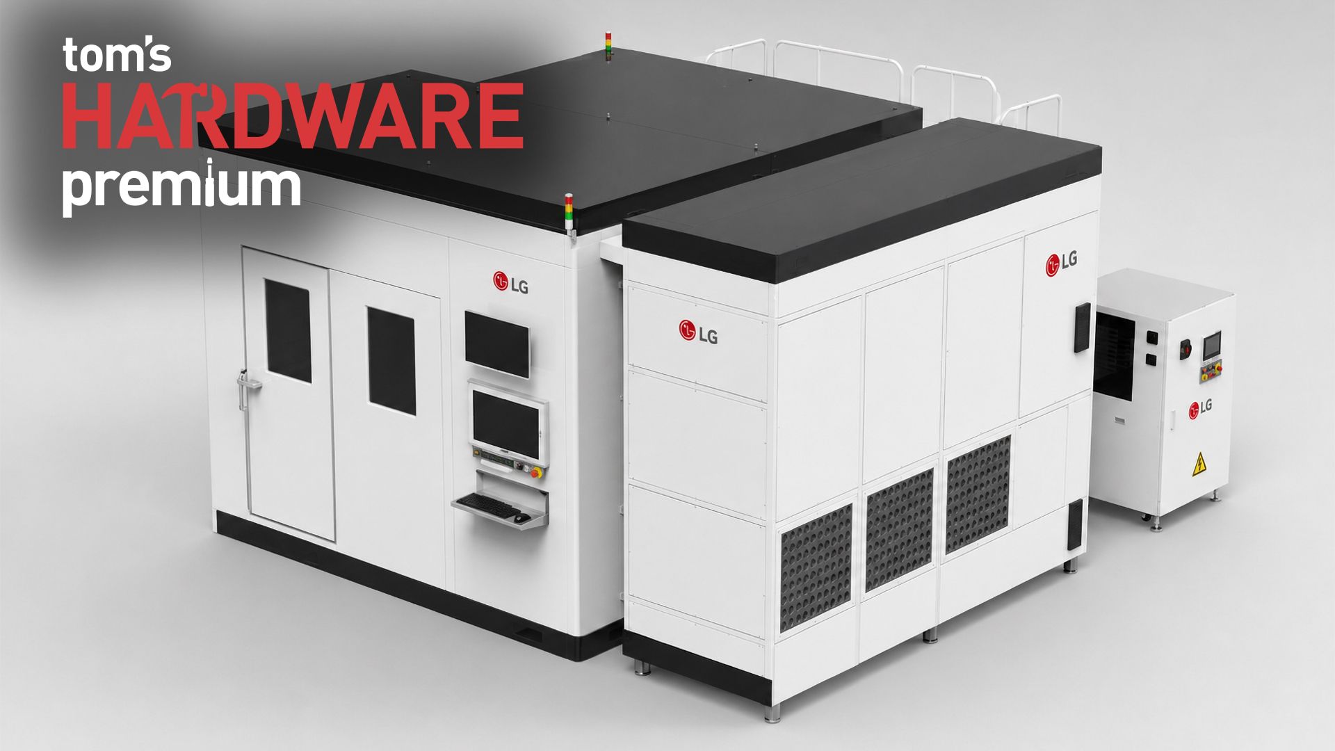
As advanced packaging technologies like EMIB and CoWoS become yet another battlefield in the semiconductor industry, outsourced semiconductor assembly and test (OSAT) companies are trying new tools in a bid to offer services that others do not. This week, LG Electronics Production Technology Institute (PRI) signed a contract with an OSAT to supply it with a maskless laser direct imaging (LDI) lithography tool that can be used to build metal-interconnect patterns in semiconductor packaging, potentially with higher yields than currently available tools, reports ETNews.LG-PRI's Laser Direct Imaging (LDI) system is a maskless lithography machine designed to pattern fine metal interconnects for advanced semiconductor packaging. While the company has developed various versions of the machine, its highest-resolution version can produce 1.5-µm line-and-space (L/S) patterns, which should be fine to 'print' wiring pitches of about 3 µm. The production equipment uses a 405-nm laser-diode light source and can process substrates as large as 600 × 600 mm, according to various media reports.
LG enters chip packaging arena with Laser Direct Imaging machine, as TSMC's CoWoS remains constrained — maskless machine is designed to pattern fine interconnects, trading resolution for higher throughput
Full Article
Original Source
Read the full article at Tomshardware →KhanList aggregates and links to publicly available news content. We do not host full articles from third-party sources. Always verify important information with original sources.