
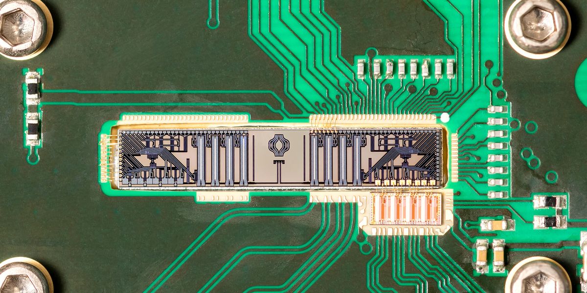
Data centers already use light in networking. Startup Optalysis aims to use specially engineered waveguides to add computational capacity to the networking path, doing math while data is in transit.The idea of computing with light has been around for over 70 years, but until recently it’s remained largely in the realm of research. Over the past few years, though, optical computing has emerged as a fast-growing industry: Market valuation of companies in this sector now totals US $2.22 billion, up from $0.4 billion in 2022. One projection suggests that the market will continue to grow exponentially in the coming years.The reason for this sudden surge will surprise no one: AI. In particular, AI inference—the process of using AI models to respond to user queries—has driven much of the construction of huge, power-hungry data centers, and relatively energy-efficient optical systems are seen as a potential way forward.“Most of the interest in [photonics] is driven by the fact that AI inference has literally become limited by power, and in a rather striking manner,” says Peter McMahon, associate professor of applied and engineering physics at Cornell University, in Ithaca, N.Y., who has researched optical computing for over a decade.Optics, at least on paper, carries the promise of doing the same math as today’s GPUs at a drastically lower level of power. Switching from electronics to optics would be a pretty radical solution. Nevertheless, like mushrooms after a rainstorm, optical-computing startups are popping up in the United States, China, Germany, and Israel. And while competing against such GPU makers as Nvidia is an ambitious goal, the investment in optical computing has spurred development of complementary approaches, such as designing alternative AI algorithms, taking on scientific computing, and enhancing in-network computing. Optalysys, based in England, is inserting optical-computing elements into the networking path, where data centers already use light. The company’s basic on-chip optical element, shown in the inset, is a Fourier transform calculator.Optalysys“I think it would be good for the technology if many of these companies made a good run at it,” says Logan Wright, assistant professor of applied physics at Yale University, in New Haven, Conn., and a former postdoc in McMahon’s lab. “I think that the technology that will be developed through this would be really, really useful, and enable photonic systems that maybe don’t get on this wave of AI but would be capable of doing really quite special things.”Optics to inference’s rescue? Inference makes up the bulk of AI energy use. The industry is already spending billions of dollars designing advanced GPUs and other chips to run inference as efficiently as possible. At the heart of the inference computation is one operation, done countless times a second: matrix-vector multiplication.Back in 1978, optical-computing pioneer Joseph W. Goodman and his coworkers proposed a method for doing matrix-vector multiplication with light. The setup was relatively simple. Let’s say a vector of length N needs to be multiplied by a matrix of size N by N. N light-emitting diodes, all in a row, encode the elements of the vector into the intensity of light—the brighter the light from an individual diode, the greater the value that diode encodes. Then, a cylindrical lens spreads out the light vertically, essentially copying the vector N times. The light then passes through an attenuator of N by N pixels. At each pixel, the light is attenuated according to the corresponding value at that location in the matrix. Passing the light through the attenuator performs the multiplication. Finally, a cylindrical lens oriented perpendicular to the first lens re-collects the light from each row, summing it up. The final vector is measured by a row of detectors. VECTOR-MATRIX MULTIPLICATION The most computationally expensive part of common AI today is vector-matrix (or matrix-matrix) multiplication. For a vector of length N (here, N = 3), it takes N2 (here, 9) multiplication steps and three accumulation steps—multiple additions at once. The argument for why optics might be advantageous over electronics goes something like this: Multiplying a matrix of size N by N by a vector of length N takes N2 multiplication steps. In electronics, each multiplication takes some energy, so the total energy used scales as N2. In optics, however, the multiplication step is passive: As long as the matrix stays the same, passing light through the attenuator costs almost no energy. The only cost is encoding the vector into light and reading out the answer, but the vector is of length N, not N2. So the energy used will scale as N, not N2, as bigger vectors and matrices are multiplied.Since Goodman’s 1978 proposal, the quality of the available optical elements has improved dramatically. Indeed, in 2022, a team of researchers at Cornell led by McMahon demonstrated an optical neural network that consumed less than one photon of energy—approximately 2.5 x 10⁻¹⁹ joules—per multiplication operation. In a standard computer, a single multiply operation can take between 10-14 and 10-12 joules, which suggests that optics could possibly reduce energy use by a factor of 100,000.But McMahon cautions against such extrapolation. First, the cost of encoding data into optics was not included in the calculation. Even if the scaling is favorable with light, in practice it’s not just the scaling that matters, it’s also the coefficients. Let’s say the energy cost of doing one multiplication with electronics is 1 picojoule, and the cost to encode one vector element with optics is 1,000 picojoules. The electronic approach still wins if the length N of the vector is fewer than 1,000 elements.McMahon says this example is not far off from reality: “One of the key questions is, How big do you have to make the system before you start winning? Lots of people have done this calculation for various kinds of neural networks. The very rough answer is somewhere between N equals 1,000 and N equals 10,000.”It’s also important to keep in mind a computing principle known as Amdahl’s law.“Amdahl’s law shouldn’t even be called a law. It’s a simple piece of common sense,” McMahon says. “If you have something that’s going to accelerate a computation, and it can accelerate 90 percent of the code, but there’s 10 percent of the code that it can’t accelerate, then the maximum possible speedup you can get is 10x.”With AI inferencing, the point is to save energy, not time. But Amdahl’s observation still applies. What fraction of today’s AI inferencing code can be better handled with optics is a complicated question that varies by approach. But it’s not 100 percent. Matrix-vector multiplication, or matrix-matrix multiplication, is only part of the inference workload—there are other, nonlinear operations that need to be performed on the data.Taking all of these caveats into account, optical-computing companies today are aiming for a 10- to 80-fold improvement in energy efficiency over today’s GPUs. The question is whether they can deliver on that promise at scale before traditional electronics catches up to those gains.Bridging the gap in free spaceThe startup Lumai, based in Oxford, England, has taken perhaps the most direct inspiration from Goodman and his team. Lumai’s head of product, Phillip Burr, declares that a free-space approach, where the light travels through air rather than on-chip waveguides, is what will enable the company’s tech to beat GPUs.Instead of the fixed attenuator used in Goodman’s proposal, Lumai is using a modern programmable device called a spatial light modulator—a pixelated membrane akin to a fancy liquid-crystal display that can modulate both the intensity and phase of light. The rest of the design is more sophisticated in practice but similar in principle to Goodman’s design: A vector is encoded into light, copied N times via a lens, passed through the spatial light modulator, collected with another lens, and the result is converted back to digital electronics. The electronics then handle the nonlinear functions. “A full vector-matrix multiply completes in a single optical cycle,” Burr says.To accurately compare the energy expenditures of the optical and GPU approaches, you must first specify which part of the workload you’re considering. Modern inference is often split into two phases: prefill, where the input query is processed and propagated through the model, and decode, where the output is generated one word (or token) at a time. Prefill is the more computationally intensive of the two. It basically involves doing vector-matrix multiplications for the same matrix over and over. Decode also involves vector-matrix multiplies, but not as intensively—the time-consuming part of decode is reading the necessary matrices in and out of memory. Vector-matrix multiplication with free-space optics Chris PhilpotThe Goodman optical computer is the simplest version of a photonic vector-matrix multiplier. Here, the vector elements are encoded into the intensity of light from three light sources, such as LEDs. Then, a cylindrical lens spreads the light vertically. The matrix elements are encoded into the opacity of an attenuator, such that when light passes through each pixel it is multiplied (attenuated) by that matrix value. Finally, another cylindrical lens collects the light horizontally, performing the accumulation step, and a photodetector measures the output vector. Lumai, and other companies in the space, are focusing on the compute-intensive prefill phase of inference. Lumai claims that its Iris Nova optical server, made available for evaluation in April 2026, is a proof of concept, and its next-generation Iris Aura server will do prefill using roughly one-tenth of the energy a GPU would use.The startup Neurophos, based in Austin, Texas, is putting a different spin on the Goodman computer design. To pack more punch into a small device, the company is leveraging its expertise in metamaterials—complex structures that can manipulate light at scales smaller than a single wavelength. The structures it has designed are bigger than a wavelength but still quite small—just several micrometers per side.“The equivalent of the optical transistor that you can get from standard silicon photonics today is like 2 millimeters long,” says Patrick Bowen, CEO of Neurophos. “You just can’t fit enough [of] them on-chip to get a compute density that remotely competes with the latest and greatest [that] TSMC [Taiwan Semiconductor Manufacturing Co.] does.”Based in Austin, Texas, Neurophos is using tiny metamaterials packed onto a chip to manipulate incoming light for efficient vector-matrix multiplication.NeurophosBowen’s team designed metamaterial-based modulators that can be programmed to manipulate the phase and intensity of light at the micrometer scale, resulting in an array of 1,000 by 1,000 modulators in a square chip with 5-mm sides. According to Bowen, Neurophos’s modulators switch over 10,000 times as fast as a standard liquid-crystal spatial light modulators do.Bowen also claims a performance advantage over Nvidia’s Blackwell GPU: “We’re targeting 50 times Blackwell B200’s speed and 35 times its energy efficiency, and have a road map to reach 250 times the speed and roughly 90 times the energy efficiency in subsequent generations.”The approach is CMOS-compatible, Bowen says, which should allow Neurophos to manufacture its chips on the semiconductor industry’s existing high-volume production lines. The company is currently choosing a site for a production facility ahead of its rack deliveries to customers in 2028.Both Lumai and Neurophos are betting they’ll get their products to market before traditional CMOS can catch up to their energy savings. “Silicon will keep improving, but digital efficiency gains now come slowly and at rising cost,” Burr says. “Optics offers a different scaling relationship, in which efficiency improves as matrices grow. Larger models, longer context windows, and agentic workloads are all pushing prefill in that direction.”Bridging the gap on-chipFree-space optics carries the promise of almost energy-free multiplication, as in Goodman’s design. But another big advance in optics since Goodman’s work in the 1970s is integrated photonics, which allows you to guide and manipulate light on-chip.“The name of the game is to do as large a vector size as possible to maximize the benefit of using optics, and for that reason the free-space approaches are promising,” says Yale’s Logan Wright. “But it’s still fundamentally harder” to use the free-space approach, “because there’s just so much less infrastructure than in silicon photonics.”Other companies—like Shanghai-based Lightelligence and Q.ANT, based in Stuttgart, Germany—are trading the 3D advantage of free-space optics for the manufacturability of photonics integrated directly onto a silicon chip.“There is a good reason that free-space optics are usually limited to 1,000 units a year,” says Q.ANT’s CEO and founder, Michael Förtsch. “The reason for this is lens inspection, assembly strategy, and so on. Semiconductor-manufacturable integrated photonic circuits are at this point way more promising to reach volume production.” Vector-matrix multiplication with integrated photonics Chris PhilpotOne way to do vector-matrix multiplication with light on-chip involves encoding vector elements into the amplitudes of pulses of light, traveling sequentially through a waveguide. The multiplication is performed by Mach-Zehnder interferometers: A waveguide splits in two, and the phase of light traveling through one of the paths is shifted by a controlled voltage. When the two paths reunite, the resulting light intensity depends on that phase shift, performing a multiplication. Encoding the matrix elements into the phase shifts turns this into vector-matrix multiplication. A photodetector then collects the light from all three pulses, performing the accumulation step.In Q.ANT’s approach, the input data is encoded into the phase and amplitude of light pulses via on-chip modulators. A vector in this scheme is represented as a sequence of such pulses, each representing one vector element. The light is guided around the chip with waveguides. The basic computational element is an interferometer: A waveguide splits into two paths, and the light beam traveling down one path is subjected to a phase shift, controlled by a set voltage. When the two paths recombine, the resulting interference performs a computation. Then, photodetectors and analog-to-digital converters turn the result back into digital data. The serialized vector-matrix multiplication approach is slower than Goodman’s computer, where the whole calculation happens at once. However, the slower speed can be mitigated by using multiple wavelengths at once, effectively encoding multiple vectors into light simultaneously.Q.ANT’s Native Processing Server is already being used in research institutions like the Leibniz Supercomputing Centre in Munich and the Jülich Supercomputing Centre in Jülich, both in Germany. Earlier this year, the company announced a commercial sale to the cloud provider Ionos. Similarly, Lightelligence’s PACE2 processor is capable of multiplying 128-by-128-element matrices. In a paper released in 2025, the company described vector-matrix multiplication at a 1-gigahertz frequency and 3-nanosecond latency, claiming two orders of magnitude lower latency than with traditional GPUs.The energy advantage is yet to be conclusively demonstrated, however, and Q.ANT’s Förtsch admits there is still a ways to go. The main issue is the energy cost of analog-to-digital conversion and back. As long as a fast, low-energy converter does not exist, Förtsch says, “we don’t see realistic chances that…a general vector-matrix multiplication machine in optics makes sense.”Beyond matrix-vector multiplicationNot everyone in the field is focused on matrix-vector multiplication, despite it being all the rage in the AI inference world. In fact, while the optical vector-matrix multiply idea goes back to the 1970s, other computations with optics have been investigated as far back as the 1950s. For example, a Fourier transform—a common operation that decomposes a complex wave or signal into its constituent frequencies—can be done in optics with a single lens.“A digital chip has to approximate [Fourier transforms] in many small steps, using hundreds to thousands of transistors and more compute cycles,” says Q.ANT’s Förtsch. “Models that use such nonlinear functions can reach the same or better accuracy with fewer parameters and fewer operations.”Even though Q.ANT’s optical processor has been used for traditional vector-matrix multiplication, the company believes its greatest advantages lie in alternative AI architectures that leverage more complex functions. “Tasks such as image classification and segmentation rely heavily on operations like Fourier series, transformations, and other nonlinear functions, which photonics handles natively. We see similar potential in generative AI, especially image and video generation,” Förtsch says.The Israel-based startup LightSolver is also targeting algorithms that are a more natural fit for its device. “If you look at propagating electromagnetic waves, essentially, they are running differential equations in their nature,” says Ruti Ben-Shlomi, CEO and cofounder of LightSolver. She says differential equations can be solved much faster and with higher energy efficiency on the company’s laser processing unit (LPU) than on a traditional computer.LightSolver’s LPU is an interesting twist on the Goodman optical-computer design. It has input light, a programmable membrane in the form of a spatial light modulator, and output light, but the whole thing is placed in a cavity, where light bounces back and forth many times before reaching a steady state. In addition, the team places a gain medium inside the cavity. This gain medium functions much like those found inside a laser, causing the bouncing light to build up in intensity. LightSolver, a startup based in Israel, is using free-space optics to quickly solve differential equations by harnessing the natural properties of light. LightSolverOnce a particular problem is encoded into the modulator, the gain medium is stimulated to emit random photons. They bounce back and forth, increasing in intensity when passing through the gain medium again, experiencing preprogrammed changes through the modulator and interacting with one another until they reach a steady state—the solution. Then, a simple camera takes a picture of the steady-state result. Using emulation, the LightSolver team recently showed that their LPU can solve differential equations 40 to 80,000 times as fast as a GPU, depending on the workflow. They are now working on explicitly benchmarking the energy improvements.LightSolver’s team is currently working on AI applications for its LPU as well, using the company’s own algorithm to do image generation from text. “We’re not doing vector-matrix multiplication very fast. We are doing something different. We need to assume that the way you train the model, and you then do inference, is completely different. But if you do it differently, you’ll be able to do image generation with dramatic energy-consumption decrease and speedup,” Ben-Shlomi says. LightSolver has a working prototype of its LPU, and the team is working on a larger, rack-mountable box.Computing in transitYet another way to leverage light’s particular strengths is being pursued by Optalysys, a startup based in Leeds, England. Nick New, founder and chief product officer, has a background in free-space optics, and so he understood that taking a Fourier transform is very easy to do with light.The key idea behind Optalysys’s technology is taking that Fourier capability of optics in free space and making it work on-chip. “Rather than using a lens these days, we have our own component, which is a passive component in the plane of the silicon that does that same job,” New says. And by cleverly designing that component with multiple outputs, the team figured out how to perform different operations as well. “Because of how the Fourier transform response is generated, you can actually pull out different mathematical operations from it,” New says. “We can produce very large, high-precision digital functions at superhigh efficiencies, using our analog photonics approach.”“We’re effectively adding processing to where there is none right now.” —Nick New, OptalysisInstead of redesigning an accelerator from scratch, Optalysys is targeting a piece of the AI workload that’s often already in the optical domain: networking. In the data center, racks of computers are connected to each other with fiber optics, and the optical connections are increasingly getting closer and closer to the GPUs and CPUs themselves.Some computations already happen while the data is en route. These computations, which include combining results from multiple GPUs, are executed inside network switch cards. But the cards naturally use power to do that math. With passive optical components, these computations could be done essentially for free.New says that in addition to communication between GPUs, Optalysys’s technology could be used to facilitate a GPU’s communication with memory, doing things like compression and format conversion on the fly. Going back to AI inference, this approach could improve the decode part of the workload. Unlike prefill, decode is memory bound: The most costly part is shuffling model data in and out of memory. “We’re more focused on the memory-bound applications, which fits very well with this principle of adding processing into the communication path,” New says. “We’re effectively adding processing to where there is none right now.”The likely future of optical computingHow likely are optical computers to replace GPUs in the data center? Yale’s Wright is not too optimistic. “The direction of algorithm development is not going to be a direction that is automatically favorable for optics,” he says. “In fact, it’s most likely to go in the opposite direction, because [AI model developers] want it to work better on GPUs.”However, even if our AI queries aren’t going to be computed in light in the next few years, that investment in the technology won’t be in vain. Says Wright, “The reason that I and many other people in the field are at least somewhat optimistic is that there’s real investment from companies like Nvidia and TSMC in developing co-packaged silicon photonics—not for computing, but for circuit switching and interconnects, and that just kind of opens the door to do a little bit more in the future.”Whether that technology ends up crunching vector-matrix multiplication, doing bespoke simulations, or performing in-network computations, the computing ecosystem seems ripe for a variety of approaches. “We see the data center of the future as heterogeneous: CPUs, GPUs and photonic NPUs [neural processing units] each take on the tasks they are best suited for,” says Q.ANT’s Förtsch. “Running each task on the most efficient hardware can significantly reduce energy use and operating costs.”
AI Is Giving Optical Computing Another Shot
Full Article
Original Source
Read the full article at Spectrum →KhanList aggregates and links to publicly available news content. We do not host full articles from third-party sources. Always verify important information with original sources.