
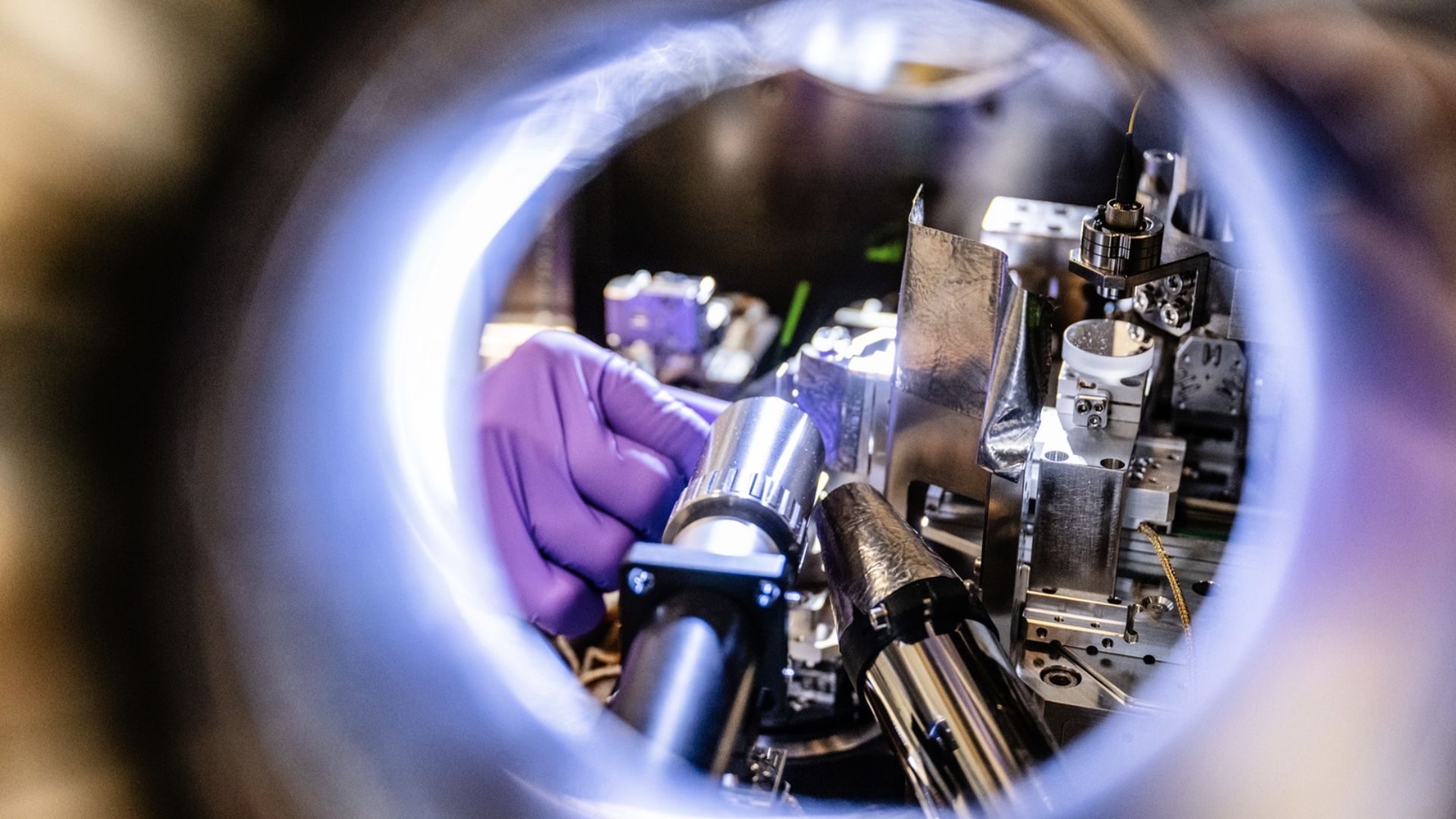
A beamline scientist with the CNM, loads a sample into the Hard X-ray Nanoprobe beamline at the APS.ANLResearchers in the United States are shaping the nanoscience frontier, using atomic‑scale control to accelerate advances in electronics, energy storage, catalysis, sensing and medicine.“At Argonne, some of the world’s brightest innovators are turning nanoscience into the next generation of discovery, pushing ideas that once seemed impossible into the realm of the achievable,” said Gary Wiederrecht, director of the Center for Nanoscale Materials and the Nanoscience and Technology division. At the nanoscale, properties can shift dramatically It has also been highlihted that modern nanoscience rests on a simple idea: Matter behaves differently when it becomes small enough. At the nanoscale, properties can shift dramatically because quantum effects and the forces acting at a material’s surface — such as electrostatic and other molecular interactions — begin to dominate their behavior.“What makes nanoscience so exciting is that it is ultimately about the extraordinary changes that occur when materials shrink from the bulk world into the nanoscale, where virtually everything begins to behave differently,” said Gary Wiederrecht, director of the CNM and Argonne’s Nanoscience and Technology division. ”At the nanoscale, new properties emerge — optical, electrical, chemical — that simply don’t exist at larger scales. Scientists and engineers use those changes to create impactful technologies that were once impossible.”Argonne entered the modern era of nanoscience with deep strengths in materials research, photon science and advanced instrumentation. For decades, its researchers have worked to develop groundbreaking tools to redefine how scientists visualize, understand and engineer matter at the atomic scale. Upgrade increased brightness of its X-ray beams 500‑fold Completed in 1995, the APS is now the world’s brightest synchrotron X‑ray source. Its comprehensive upgrade, completed in 2026, increased the brightness of its X-ray beams 500‑fold, enabling researchers to more precisely image atomic structures and track defect formation in real time as materials undergo different environmental stresses, according to a press release.A powerful new tool, Argonne’s world‑class In Situ Nanoprobe (ISN), moves the lab’s beamline imaging capability into the realm of “in situ” study, where researchers can watch how materials work, adapt and fail in real‑world conditions. This is a critical step toward breakthroughs in energy, microelectronics, quantum systems and advanced manufacturing.“The APS is already one of the world’s great engines for understanding matter,” said Sarah Wiegold, an Argonne physicist. ”The ISN expands that strength by adding an especially important dimension: the ability to probe nanoscale behavior under realistic operating conditions.”The ISN connects with complementary APS techniques that examine materials across larger length scales, different time scales and alternate modes of contrast. Together, these capabilities create a far more complete understanding of complex materials — from the atomic and nanoscale origins of behavior to system-level performance, as per the release.Get the latest in engineering, tech, space & science - delivered daily to your inbox.Prabhat, an alumnus of the Indian Institute of Mass Communication, is a tech and defense journalist. While he enjoys writing on modern weapons and emerging tech, he has also reported on global politics and business. He has been previously associated with well-known media houses, including the International Business Times (Singapore Edition) and ANI.
US lab’s 500-times brighter X-rays can track material’s defect formation in real time
Full Article
Original Source
Read the full article at Interestingengineering →KhanList aggregates and links to publicly available news content. We do not host full articles from third-party sources. Always verify important information with original sources.