
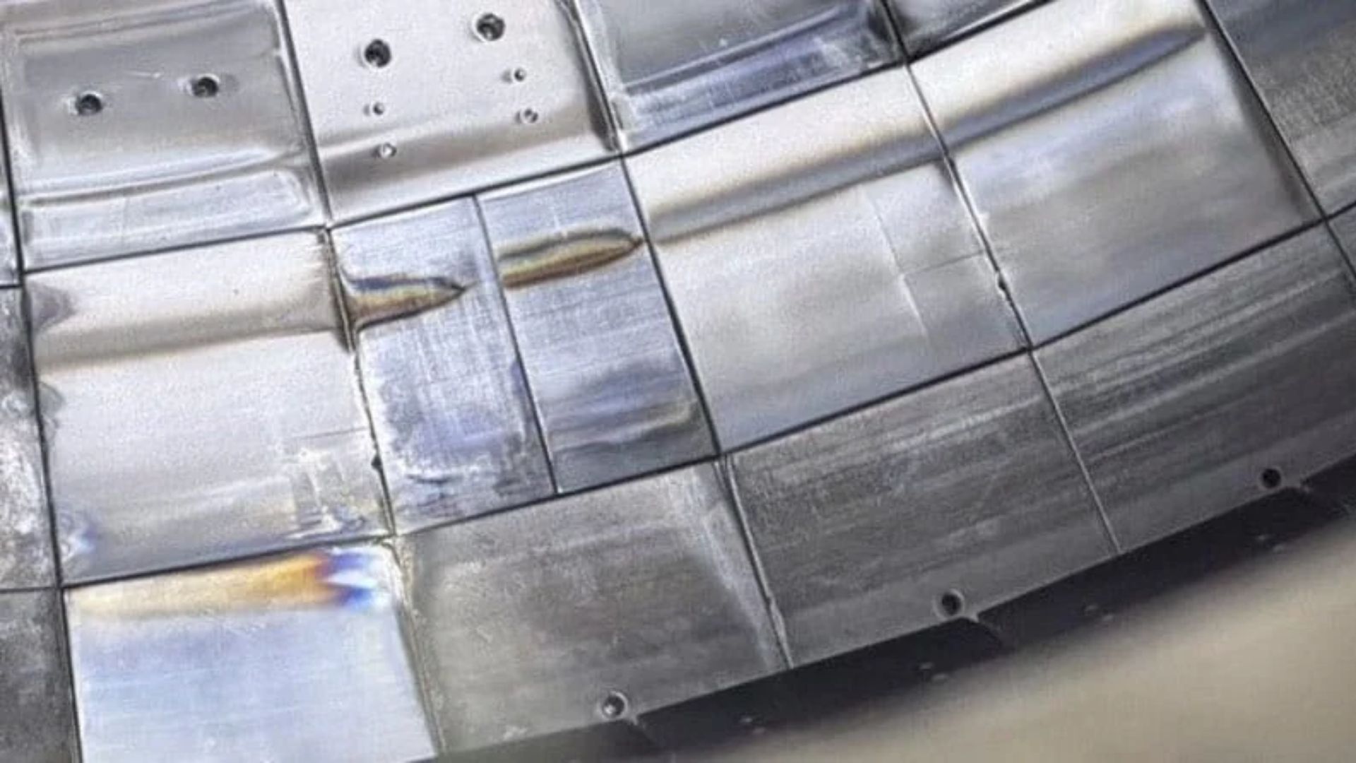
Full-size 3D-printed tungsten tiles have survived extreme heat inside a major nuclear fusion test reactor and emerged completely intact. The protective components endured 74 direct plasma discharges inside the DIII-D National Fusion Facility in San Diego. The tests subjected the tiles to three days of punishing particle bombardment in the machine’s exhaust zone, called the divertor. During high-power runs, the tiles clocked roughly four minutes of direct plasma exposure. They even survived an accidental trial by fire when a neighboring, traditional tile melted and sprayed liquid metal across them. The printed surfaces held firm, proving the material can withstand the intense heat flux and particle bombardment driven by plasma that is hotter than the center of the Sun. Tungsten is the premier choice to line future fusion power plants like ITER. It boasts the highest melting point of any metal at 3,422°C (6,191°F), more than twice that of steel. It is also exceptionally dense, weighing about as much as pure gold. Yet tungsten has long frustrated engineers. Below 600°C (1,112°F), the metal becomes brittle and shatters like glass under physical stress. “However, most attempts to 3D print tungsten, nearly all using lasers as the heat source for printing, have ended up porous and riddled with cracks,” said the team. Using a high-speed electron beam To overcome this hurdle, researchers turned to electron-beam powder bed fusion (EB-PBF). This method uses a high-speed electron beam to melt tungsten powder layer by layer inside a vacuum chamber. The beam sweeps across the powder bed quickly enough to keep the surrounding metal above 1,400°C (2,552°F) during the entire build. By keeping the build envelope red-hot throughout the process, the system prevents cracking caused by thermal shock and brittle cooling during fabrication. While researchers proved the concept on small coin-sized samples in 2025, building reactor-ready components required an industrial scale-up. The final tiles needed to measure roughly 140 millimeters across and 20 millimeters thick. A joint team from North Carolina State University, Oak Ridge National Laboratory (ORNL), and Japanese precision manufacturer JEOL Ltd pulled off the leap in just eight months. JEOL fabricated the full-scale tiles on its large-format printer in Akishima, Japan. ORNL provided fusion materials expertise and project funding. Removing a critical bottleneck Once printed, the tiles were shipped to NC State for finishing. Engineers shaped the mounting fixtures using electrical discharge machining, an electrical wire-cutting method that introduces no mechanical strain. A computer-controlled grinder then removed roughly 250 microns from the surface, creating a mirror-like finish tailored to the divertor’s curved walls. The tiles were mounted on copper-alloy pedestals and bolted into the reactor for testing in July. Scientists say the successful trial removes a critical bottleneck on the road to commercial fusion energy. By demonstrating that large-format additive manufacturing can produce robust, crack-free tungsten parts, the team showed that advanced 3D printing is no longer just an experimental curiosity, but a viable factory method for building the next generation of clean fusion reactors. “Qualifying new materials and manufacturing methods requires fusion-relevant data,” concluded Dr. Florian Laggner, an assistant professor and plasma physicist in NC State’s Department of Nuclear Engineering. “By exposing additively manufactured tungsten in DIII-D, we are generating that data on survivability and erosion.” Get the latest in engineering, tech, space & science - delivered daily to your inbox.An active and versatile journalist and news editor. He has covered regular and breaking news for several leading publications and news media, including The Hindu, Economic Times, Tomorrow Makers, and many more. Aman holds expertise in politics, travel, and tech news, especially in AI, advanced algorithms, and blockchain, with a strong curiosity about all things that fall under science and tech.
Tungsten 3D-printed at 2,552°F survives 74 plasma blasts in US nuclear fusion reactor
Full Article
Original Source
Read the full article at Interestingengineering →KhanList aggregates and links to publicly available news content. We do not host full articles from third-party sources. Always verify important information with original sources.