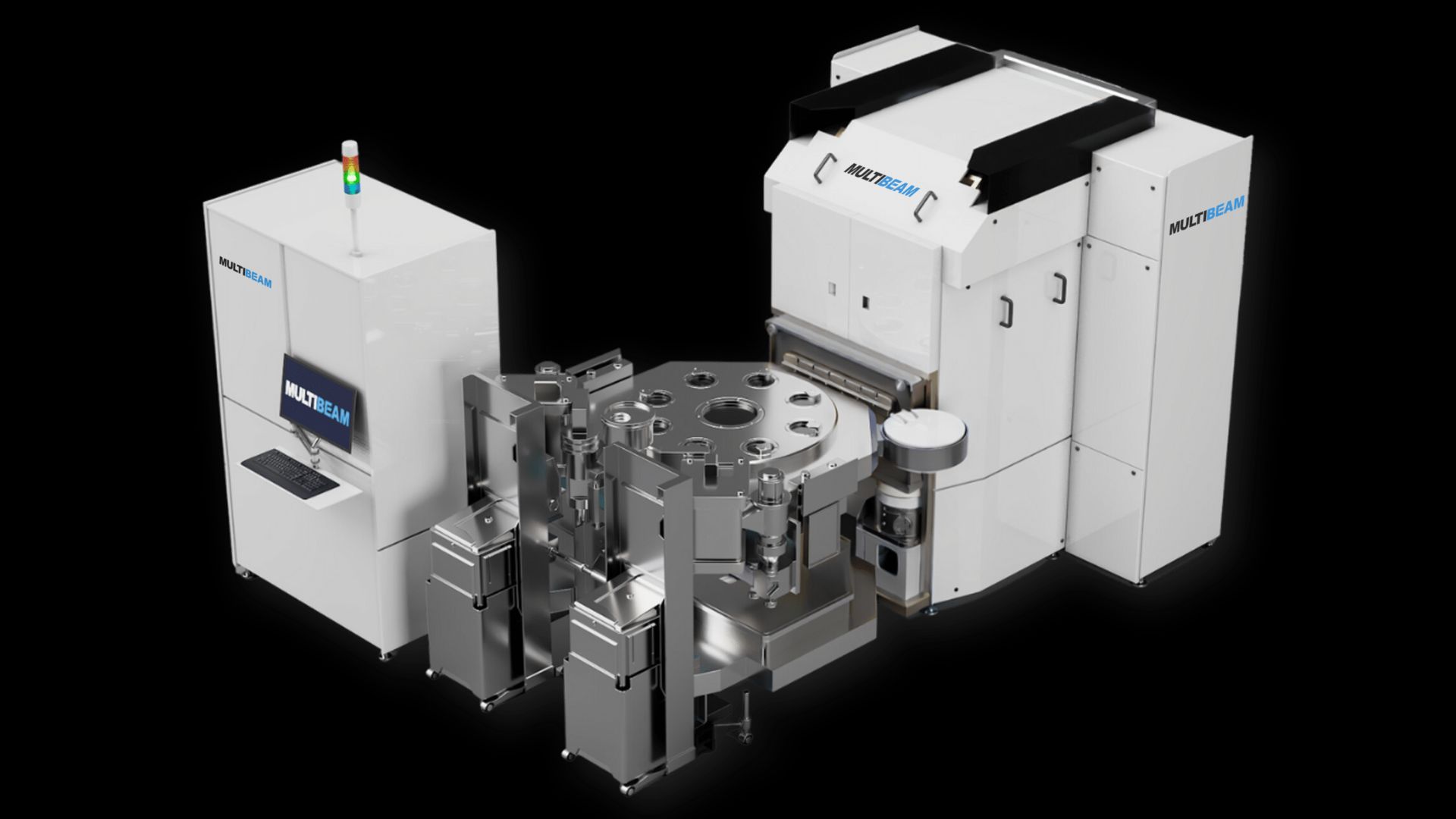
Multibeam Corp. has secured its first order from Taiwan after National Tsing Hua University (NTHU) selected the company’s newly launched MBX multi-column electron beam lithography (EBL) platform for advanced semiconductor research and process development. The system will be installed at NTHU’s College of Semiconductor Research (CoSR) and used for academic research as well as joint development projects with Taiwan’s semiconductor industry. Delivery is scheduled for 2027, marking Multibeam’s first deployment in the world’s largest semiconductor manufacturing ecosystem. NTHU selects MBX for next-generation chip research According to Multibeam, the MBX platform will support the development of manufacturing processes for advanced chip integration, helping researchers accelerate the transition of new semiconductor designs from laboratory concepts to production-ready technologies. The company said the system was selected following an evaluation of its capabilities for high-resolution, maskless electron beam lithography, particularly for advanced packaging applications such as chip-first and chip-last integration as well as large-format interposers. Unlike conventional lithography systems that rely on photomasks, the MBX platform enables researchers to directly write circuit patterns onto wafers. This allows new chip layouts to be fabricated immediately after design completion, eliminating the need to manufacture masks for every design iteration and significantly shortening research and development cycles. Why electron beam lithography matters Electron beam lithography has long been valued for its exceptional resolution, but conventional single-beam systems have generally been too slow for many high-throughput manufacturing applications. Multibeam’s approach uses multiple electron beams operating simultaneously, increasing throughput while maintaining the precision needed for advanced semiconductor fabrication. According to the company, the platform delivers high critical-dimension uniformity, low line-edge roughness, and a large process window across an entire wafer. These capabilities are becoming increasingly important as semiconductor manufacturers pursue advanced packaging, heterogeneous integration, photonics, quantum computing, and custom AI accelerators, all of which require increasingly complex chip architectures that can be difficult or prohibitively expensive to produce using conventional optical lithography. The system is also designed to support rapid experimentation by allowing multiple device variants to be fabricated on a single wafer, enabling researchers to evaluate different designs in parallel while reducing development time and manufacturing costs. Supporting Taiwan’s semiconductor ecosystem NTHU described the new system as an important addition to its semiconductor research infrastructure. Professor Burn Lin, Distinguished Research Chair at NTHU, said the university aims to accelerate the development of next-generation semiconductor technologies while training engineers for Taiwan’s globally significant chip industry. He added that the MBX platform’s combination of higher throughput, greater patterning flexibility, and improved precision made it well suited to the university’s research programs in advanced packaging, photonics, and quantum computing. For Multibeam, the order represents more than a single system sale. Taiwan produces the majority of the world’s advanced semiconductors, making it one of the industry’s most strategically important markets. Establishing its first installation there could provide the company with opportunities to demonstrate its second-generation lithography platform to one of the world’s most concentrated semiconductor ecosystems. The deployment will also expand Multibeam’s installed customer base, which already includes SkyWater Technology, where the company’s electron beam lithography technology is being used for advanced integration, photonics, quantum computing, and rapid prototyping applications. As demand grows for application-specific chips and increasingly sophisticated semiconductor packaging driven by artificial intelligence and high-performance computing, technologies capable of reducing development cycles while enabling more flexible manufacturing workflows are expected to play an increasingly important role in next-generation chip production. Recommended ArticlesGet the latest in engineering, tech, space & science - delivered daily to your inbox.Kaif Shaikh is a journalist and writer passionate about turning complex information into clear, impactful stories. His writing covers technology, sustainability, geopolitics, and occasionally fiction. A graduate in Journalism and Mass Communication, his work has appeared in the Times of India and beyond. After a near-fatal experience, Kaif began seeing both stories and silences differently. Outside work, he juggles far too many projects and passions, but always makes time to read, reflect, and hold onto the thread of wonder.
Taiwan adopts US firm`s chipmaking system that prints circuits without photomasks
Full Article
Original Source
Read the full article at Interestingengineering →KhanList aggregates and links to publicly available news content. We do not host full articles from third-party sources. Always verify important information with original sources.