
Rigaku and Tohoku University have opened a research institute aimed at expanding what X-ray metrology can measure inside advanced semiconductor structures. The Rigaku-Tohoku University Co-Creation Research Institute for X-ray Metrology started on August 1 at Tohoku University in Sendai, Japan. The partners will work together for an initial three years, with an extension possible based on research results. The timing reflects a growing measurement problem in chip manufacturing. Devices now contain smaller features, more layers, and increasingly diverse materials. Engineers need to inspect those structures without cutting them apart or damaging them. Conventional X-ray techniques cannot always resolve the smallest structures or accurately capture changes through multilayer devices. The new institute will explore approaches that could extend those capabilities. As chip architectures become denser, measurements also need to distinguish structures buried beneath multiple material layers. That makes both the X-ray measurement itself and the interpretation of its data increasingly demanding. Soft X-rays enter the picture One major research direction involves soft X-rays, which have lower energy and longer wavelengths than conventional X-rays. Tohoku University brings a major advantage to the effort through NanoTerasu, its next-generation synchrotron radiation facility. Researchers can use its capabilities to investigate structures that challenge conventional measurement methods. The university will also contribute expertise in information science. That matters as X-ray measurements generate increasingly complex datasets that require sophisticated analysis. Rigaku brings its experience developing X-ray analytical systems and metrology technologies. The partners will combine those capabilities to develop new measurement methods and improve data interpretation. Initial research will focus heavily on semiconductor applications. The institute will examine microstructure measurement using soft X-rays while advancing information science techniques for X-ray analysis. The work could eventually support measurements across other advanced materials. Electronic and functional materials also require detailed information about microscopic structures and material states. Researchers are part of the plan Technology development represents only half of the institute’s mission. The partners also want to train researchers and engineers who can work across advanced X-ray metrology. Planned education will span fundamental X-ray principles through applications involving new materials and structures. The institute also aims to introduce credit-bearing university courses. Graduate students can receive support through the Rigaku Scholarship System. The scholarships will support X-ray-related research and help connect academic work with practical measurement applications. Kazuhiko Omote, general manager of Rigaku’s X-ray Research Laboratory, said the field still has room for discoveries despite more than 130 years of X-ray research. “I am convinced that X-rays still hold numerous possibilities that have yet to be revealed,” Omote said. He added that the next generation will play an important role in uncovering them. Daichi Chiba, director of Tohoku University’s International Center for Synchrotron Radiation Innovation Smart, sees the institute as a meeting point between disciplines. He said the goal extends beyond combining Rigaku’s technology with NanoTerasu. The institute also aims to create an environment where researchers from different generations and fields can develop new ideas together. Its first three years will concentrate on soft X-ray metrology for semiconductors and advanced X-ray data analysis. The resulting research will help determine how the institute expands into electronic materials, functional materials, and other areas requiring precise structural characterization. Get the latest in engineering, tech, space & science - delivered daily to your inbox.Aamir is a seasoned tech journalist with experience at Exhibit Magazine, Republic World, and PR Newswire. With a deep love for all things tech and science, he has spent years decoding the latest innovations and exploring how they shape industries, lifestyles, and the future of humanity.
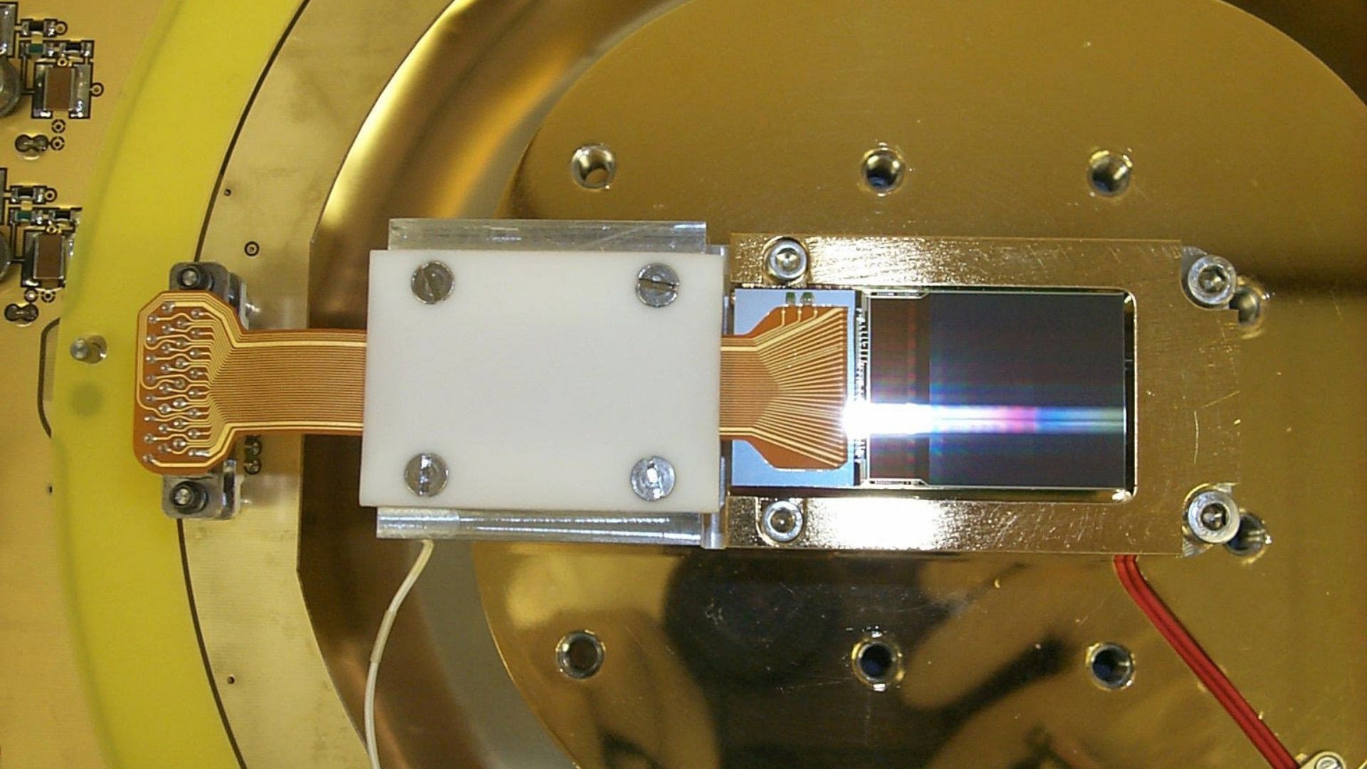
Semiconductor X-ray metrology exposes buried microscopic flaws in multilayer chips
Full Article
Original Source
Read the full article at Interestingengineering →KhanList aggregates and links to publicly available news content. We do not host full articles from third-party sources. Always verify important information with original sources.