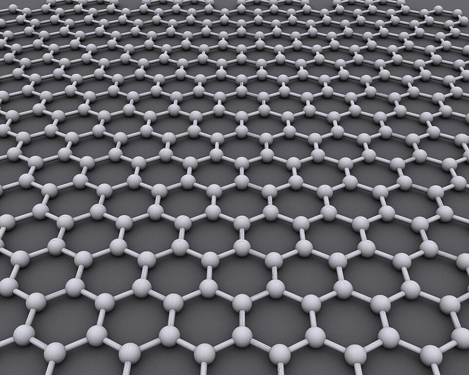
Researchers from Peking University have developed a better way to make a special kind of graphene-based quantum material. If scaled and refined further, this discovery could pave the way for making quantum computers more practical in the future. According to their study, the team has found a way to reliably fabricate rhombohedral graphene at a purity and size not yet achieved. This form of graphene, the team explains, is highly prized as it can host exotic quantum states while remaining stable. Ordinarily, graphene consists of sheets stacked in alternating offset “piles” with something called ABCABC stacking (also called rhombohedral) considered the best. In this setup, the sheets shift in the same direction before repeating, which is great but rare and unstable since they have an annoying tendency to degrade into more stable ABAB stacking when left to their own devices. In rhombohedral sheets, electrons radically change how they behave within the structure. According to the team, such electrons interact unusually strongly and can form collective quantum states, including superconducting and “quantum Hall phases.” Clever stacking for quantum computing This could make them useful as “topological” qubits that could be encoded with the overall state of a system rather than one fragile local particle. That could make it intrinsically more resistant to noise, one of the central obstacles in quantum computing. Before the team’s breakthrough, researchers essentially had to peel graphite apart with tape and search through flakes until they found one with the correct stacking. Fewer than 1% reportedly had it. That is perfectly adequate for individual physics experiments, but clearly not ideal as a manufacturing method. “Basically peeling off flakes with tape and then hunting under a microscope for the rare few that happened to have the right stacking, which made up less than 1 percent of the samples,” study co-author Zhang Zhibin explained. The new fabrication method, however, is able to “grow” ABC sheets in a controlled process. To achieve this, they took an aluminum-oxide surface with a microscopic step to guide the stacking. To this, a copper–nickel alloy is added that acts as both catalyst and growth template. Then high temperatures are used to make carbon assemble into graphene, with a final step added to “force” successive layers to remain displaced in the ABC sequence. And the results are impressive. “The samples we produced are over 99 percent pure, with maximum dimensions of 160 by 80 micrometers and thickness up to 120 nanometers,” study lead Liu Kaihui said. “We can tune the number of layers from several dozen to several hundred as needed,” Kaihui added. More work to do Liu explained to the South China Morning Post (SCMP) that the material offers “an excellent platform for studying quantum phenomena and, compared to similar materials, it is abundant and easy to process”. “We can’t predict how far this material will go, but material preparation is the foundation for further research. If future applications emerge, we’ll be ready to build the next generation of quantum devices,” he added. “Two-dimensional materials already have mature applications in acoustic films and thermal conductors for lithography machines,” he added. “In chips, while we haven’t seen large-scale replacement of silicon or silicon carbide, there is growing research into integrating 2D materials into the most critical parts – like the most energy-hungry sections of AI chips or the highest-density areas of memory chips – to leverage their unique advantages,” he said. Looking ahead, the team plans to stitch smaller pieces of rhombohedral graphene together to produce larger, device-ready sheets. Recommended ArticlesGet the latest in engineering, tech, space & science - delivered daily to your inbox.Christopher graduated from Cardiff University in 2004 with a Masters Degree in Geology. Since then, he has worked exclusively within the Built Environment, Occupational Health and Safety and Environmental Consultancy industries. He is a qualified and accredited Energy Consultant, Green Deal Assessor and Practitioner member of IEMA. Chris’s main interests range from Science and Engineering, Military and Ancient History to Politics and Philosophy.
Rare 99% pure graphene produced in China for advanced quantum chips, semiconductors
Full Article
Original Source
Read the full article at Interestingengineering →KhanList aggregates and links to publicly available news content. We do not host full articles from third-party sources. Always verify important information with original sources.