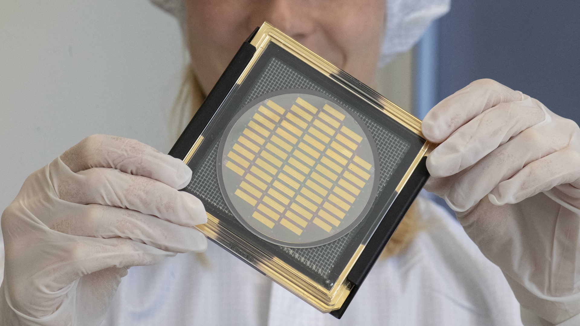
Researchers in the US have unveiled a new photonics design platform that could speed up the development of high-performance chips for data centers and other advanced optical systems. California-based semiconductor company OpenLight and Israeli chipmaker Tower Semiconductor have expanded their PH18DA photonics ecosystem by unveiling OpenLight’s photonic Process Design Kit (PDK). It is now available via Cadence’s electronic design automation (EDA) tools. The open-platform design kit provides engineers with a comprehensive library of active and passive components for building custom Photonic Application-Specific Integrated Circuits (PASICs). It also makes it possible to build photonic integrated circuits (PICs) with a widely adopted chip design environment. This could simplify and accelerate the development of new photonic chips. The technology can be utilized for 400G and 1.6T photonic circuits. “This integration simplifies adoption and strengthens the path from design to production on the PH18D platform,” Adam Carter, PhD, OpenLight CEO, said. Adding lasers to chips The technology is reportedly based on Tower Semiconductor’s PH18DA platform, which combines indium phosphide (InP) with silicon. InP is a critical compound semiconductor material. It is used to generate and detect laser light in high-speed optical communications and AI data center infrastructure. The platform allows active photonic parts, like lasers, modulators and amplifiers, to be integrated into a single monolithic photonic chip. This could make it easier to build compact and high-performance optical systems. “By making our PDK available on Cadence tools, we enable customers to design photonic integrated circuits within the same environment they rely on for advanced IC development,” Carter emphasized. According to the team, the technology could be utilized for optical connections, smart infrastructure, as well as sensors. Moreover, the wider ecosystem combines OpenLight’s photonics technology with Tower’s chip manufacturing expertise and Cadence’s design tools. It also makes photonic chip development more similar to the established process used to design conventional electronic integrated circuits. Gilles Lamant, Cadence engineer, said the addition of the PH18DA PDK to its photonics ecosystem brings integrated active devices into high-performance electro-optical designs. Aiming for 1.6T connections With the platform, the companies are targeting 400G and 1.6T laser-integrated photonic circuits. The technology could support advanced near-packaged optics (NPO) and co-packaged optics (CPO). “This approach enables customers to streamline development of 400G and 1.6T laser-integrated photonic integrated circuits, while achieving co-optimized PIC and EIC designs for improved performance, power efficiency, and scalability necessary for next-generation near- and co-packaged optics solutions,” Samir Chaudhry, PhD, Tower Semiconductor’s VP of customer design enablement, said in a press release. The expanded ecosystem should provide a more direct path from chip design to manufacturing by bringing photonics technology, design tools, and production capabilities together. “In collaboration with Cadence and OpenLight, we are advancing design capabilities on the PH18DA platform through a new capability that integrates expertise across technology, IP, and ED,” Chaudhry added.“Adding the OpenLight PDK PH18DA manufactured by Tower Semiconductor to the rich portfolio of photonics processes supported by the Cadence Photonics ecosystem is a key milestone because it marks the introduction of integrated active devices for high-performance, co-optimized electro-optical designs,” Lamant concluded. Recommended ArticlesGet the latest in engineering, tech, space & science - delivered daily to your inbox.Based in Skopje, North Macedonia. Her work has appeared in Daily Mail, Mirror, Daily Star, Yahoo, NationalWorld, Newsweek, Press Gazette and others. She covers stories on batteries, wind energy, sustainable shipping and new discoveries. When she's not chasing the next big science story, she's traveling, exploring new cultures, or enjoying good food with even better wine.
New US smart platform speeds development of 1.6T photonic chips for data centers
Full Article
Original Source
Read the full article at Interestingengineering →KhanList aggregates and links to publicly available news content. We do not host full articles from third-party sources. Always verify important information with original sources.