
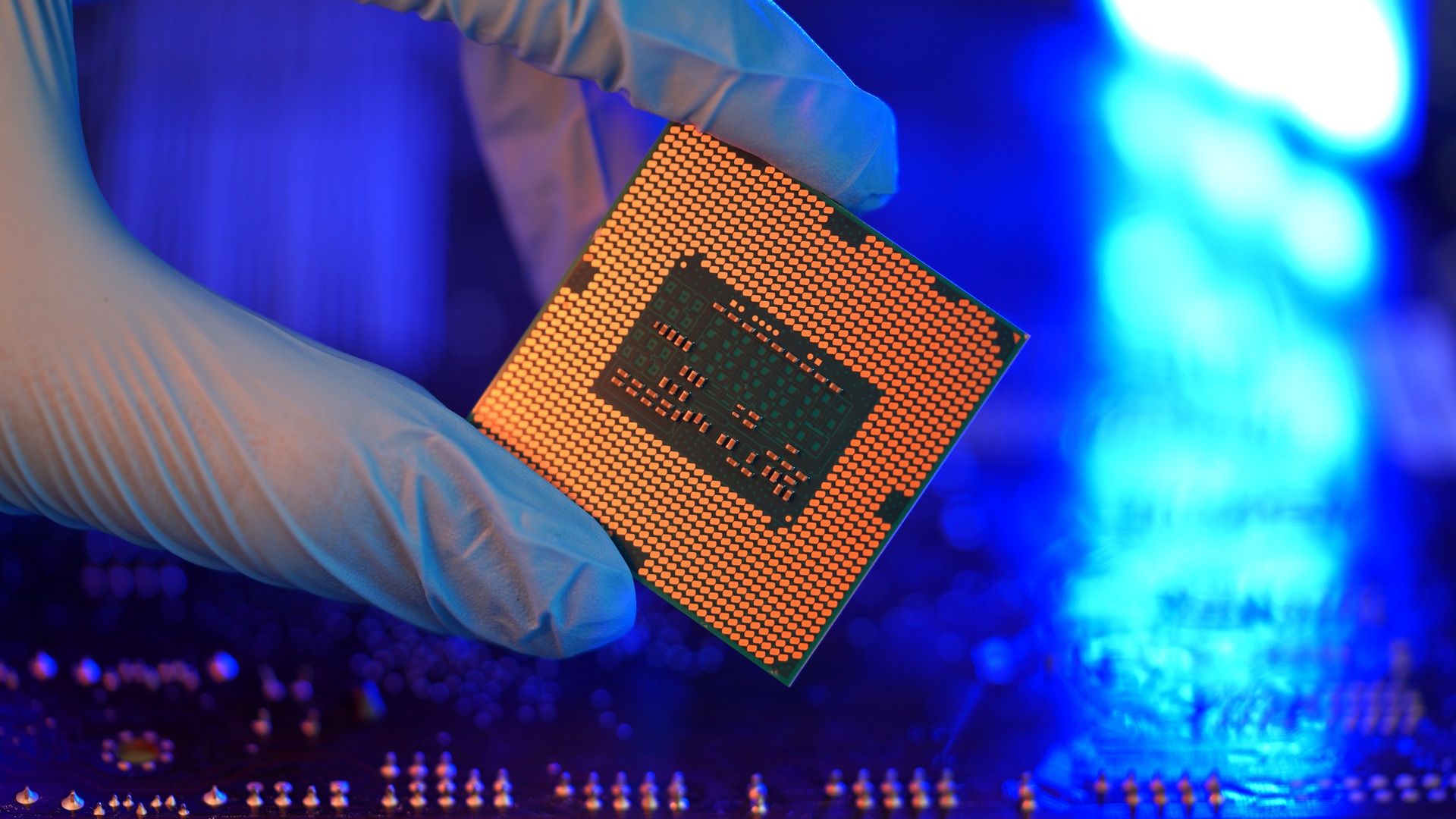
Huawei says a new vertically stacked semiconductor design can address one of the biggest problems facing its next-generation smartphone chips: heat. The company has published new measurements for its Tau Scaling Law-based architecture, claiming that a coming Kirin processor can increase transistor density while using less power and running cooler than its predecessor. The findings could be important for Huawei as it works to improve chip performance despite China’s limited access to advanced semiconductor manufacturing equipment. The research was led by He Tingbo, chairwoman of the Huawei Scientist Committee and president of the company’s semiconductor business department. The paper argues against concerns that stacking logic circuits vertically would create a thermal bottleneck that could prevent the technology from being used in high-performance mobile processors. According to the paper, the new Kirin chip has 55% more transistors per square millimetre than the Kirin 9030 Pro. It can also reduce power consumption by as much as 66% for some key workloads. Vertical stacking cuts heat The approach is based on Huawei’s LogicFolding architecture, which stacks active chip layers vertically instead of placing all the circuitry across a conventional two-dimensional layout. That arrangement shortens the distance that signals need to travel between processing components. Huawei says this can reduce energy losses in neural processing units, graphics processing units, central processing units and digital signal processors, all of which contribute significantly to a smartphone processor’s power and thermal load. The company also used thermal planning to spread heat more effectively across the chip. According to Kaiyuan Securities, Huawei reduced source power density through folding and positioned the most heat-intensive modules along paths where heat can escape more easily. The brokerage said, “The new chip reduces power consumption while increasing transistor density, allowing it to flexibly switch between functional constraints and peak performance.” A workaround for constraints Huawei’s approach is particularly significant because it is being developed under restrictions that limit China’s access to the most advanced chipmaking tools. The company’s Tau Scaling Law, unveiled in May, proposes a different route to increasing transistor density without relying on cutting-edge extreme ultraviolet lithography. Huawei has claimed that LogicFolding could eventually deliver transistor densities comparable to those associated with 1.4-nanometre manufacturing processes by 2031. Its latest paper provides another set of production-related measurements supporting that direction. The company has now published three papers on the Tau Scaling Law since May. A paper released in July said the upcoming smartphone processor was on track for a 55% transistor-density increase over the Kirin 9030 Pro. The latest findings also point to a broader push around chip packaging and three-dimensional integration. Analysts expect the technology to encourage work on new semiconductor materials, packaging methods and equipment that could help Chinese chipmakers improve performance without relying entirely on foreign manufacturing technology. Zheng Lei, chief economist at Samoyed Cloud Technology Group, described the approach as “born out of necessity” but said there was still room for development. He also expects the new Kirin processor to address its overheating challenges through the method. The results could therefore matter beyond Huawei’s next smartphones. If the claimed combination of higher density, lower power consumption and improved thermal management holds up under independent testing, vertically integrated chip designs could become a more important way to extract performance when conventional scaling becomes harder.The study was published on ChinaXiv, a platform for scientific papers that have not yet undergone peer review.Get the latest in engineering, tech, space & science - delivered daily to your inbox.With over a decade-long career in journalism, Neetika Walter has worked with The Economic Times, ANI, and Hindustan Times, covering politics, business, technology, and the clean energy sector. Passionate about contemporary culture, books, poetry, and storytelling, she brings depth and insight to her writing. When she isn’t chasing stories, she’s likely lost in a book or enjoying the company of her dogs.
Huawei’s new chip design tackles overheating with 55% higher transistor density
Full Article
Original Source
Read the full article at Interestingengineering →KhanList aggregates and links to publicly available news content. We do not host full articles from third-party sources. Always verify important information with original sources.