
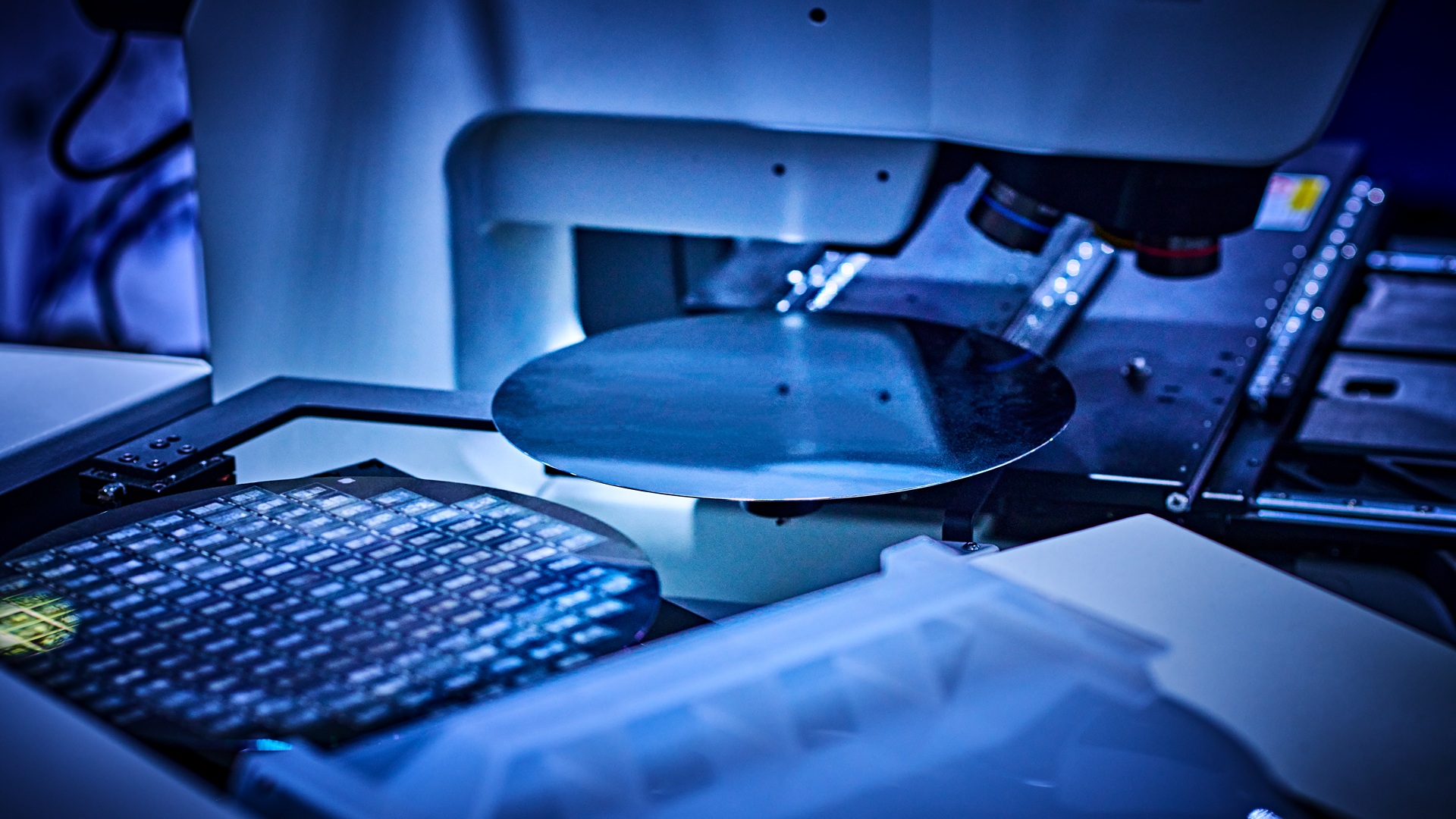
Silicon-photonics chips can move data using light instead of electrical signals, but conventional versions are rigid and opaque. MIT researchers have now developed a way to make these chips both flexible and transparent, while using semiconductor manufacturing methods that can work across large wafers. The new process could make silicon photonics useful in applications where rigid chips do not fit. Potential uses include health monitors that conform to the body and augmented-reality displays built into curved surfaces such as aircraft pilot visors. The researchers developed the process with engineers at NY Creates’ Albany NanoTech Complex. Instead of producing individual flexible or transparent devices in the laboratory, their approach creates 300-millimeter wafers containing the optical structures needed for silicon photonics. The resulting chips are only a few microns thick. Tests showed that a chip could be bent thousands of times around cylinders of different sizes, including one roughly as wide as a small screw, without losing performance. Chips built for bending The manufacturing process starts much like that used for conventional silicon wafers. Researchers deposit and pattern optical waveguides, which act as tiny pathways for light, on a silicon substrate. A temporary silicon wafer is then bonded to the structure before the original silicon substrate is removed. This leaves behind the oxide and waveguiding layers. The researchers attach a thin, transparent polyester film to the remaining structure before removing the temporary support. The result is a thin wafer that can bend while allowing light to pass through it. “Because we are using stable 300-millimeter foundry fabrication tools, we can design systems with a very large number of devices and feel confident that they are going to perform up to specifications, which is extremely important,” lead author Tal Sneh says. Getting to that point required careful control of stress during fabrication. Removing most of the silicon from a large wafer can cause it to bow or develop ripples, potentially damaging the ultrathin layers. The team kept fabrication temperatures at or below 500 degrees Celsius to manage this stress. It also combined industrial silicon-thinning methods with a more selective chemical etching process for the final material removal. Transparent enough for displays The researchers then tested whether the new platform could maintain its optical performance while being flexible and transparent. In bending experiments, the chip showed no performance degradation after thousands of bends around small cylinders. It only began to degrade when bent around a toothpick several times. The team also tested transparency using a bionic-eye setup. The chip produced minimal haze and did not noticeably distort images viewed through it, suggesting that the material could work in optical systems placed directly in front of the eye. That could enable curved augmented-reality displays integrated into windshields or pilot visors. Such systems could potentially replace some of the bulky optical components currently used to provide pilots with real-time information. The researchers also see possibilities for discreet wearable devices that need to follow the contours of the human body. “We’ve now developed a wafer-scale process that produces wafers that are mechanically flexible and optically transparent, enabling novel applications that weren’t previously possible with silicon photonics. We hope that, by working closely with our colleagues at NY Creates and using the foundry at the Albany NanoTech Complex, there’s the potential for us to make the platform accessible to other groups within our research community and open these new application areas to the field of silicon photonics as a whole,” says Jelena Notaros, senior author of the study. The researchers plan to add more complex components, improve waveguide efficiency, and further increase transparency as they develop the platform. The study is published in the journal Optica. Get the latest in engineering, tech, space & science - delivered daily to your inbox.With over a decade-long career in journalism, Neetika Walter has worked with The Economic Times, ANI, and Hindustan Times, covering politics, business, technology, and the clean energy sector. Passionate about contemporary culture, books, poetry, and storytelling, she brings depth and insight to her writing. When she isn’t chasing stories, she’s likely lost in a book or enjoying the company of her dogs.
300-mm wafers enable transparent chips that bend thousands of times without failing
Full Article
Original Source
Read the full article at Interestingengineering →KhanList aggregates and links to publicly available news content. We do not host full articles from third-party sources. Always verify important information with original sources.